本文PLL的基础内容参考了Digital Integrated Circuits一书,下载方式:在 vdoc 搜索关键字 Digital Integrated Circuits
PLL的应用概述
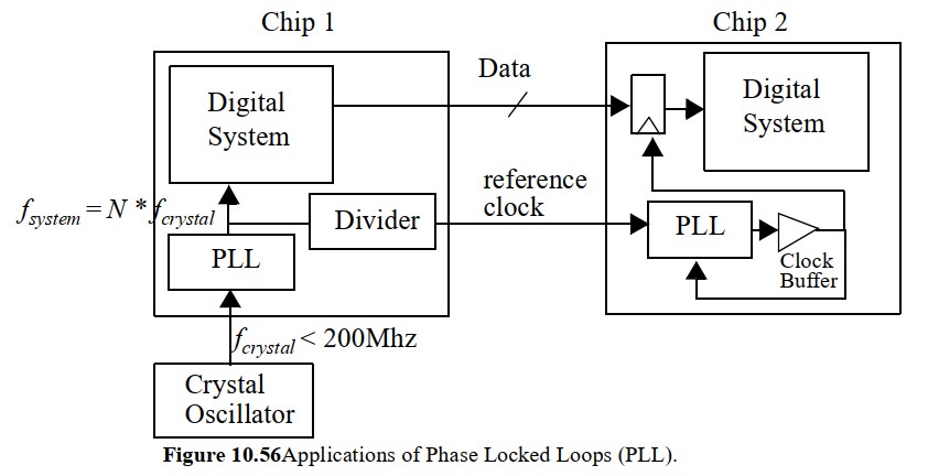
两个作用:Clock Synthesis(时钟综合)和 Clock Synchronization(时钟同步)
- Clock Synthesis,Synthesis是综合/生成的意思,Clock Synthesis即生成时钟,但此处含义不是作为时钟源,而是在低频晶振时钟的基础上倍频生成高频时钟:其中低频的晶振时钟的特性:10~200MHz, accurate, low-jitter ,高频时钟特性:200MHz ~ GHz级别,通常也称为系统时钟,例如SOC core的基准频率
- Clock Synchronization,不同芯片之间传递时钟信号需要同步时钟相位,例如SOC的CPU和外设之间的通信接口一般是:分频后的时钟信号(reference clock)和数据信号(Date),CPU和外设间的信号传递是需要时间的,高速信号传递到外设侧有相位偏移(可以简单理解为延迟),因此需要PLL同步时钟相位以保证对数据采样的正确性(想象一下,如果reference clock相位偏移过大,可能每个采样时刻得到的data数据都是错位的)
相位的概念
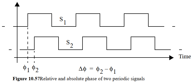
Digital Integrated Circuits一书对相位的描述:
Periodic signals of known frequency can be discribed exactly by only one parameter, their
phase. More accurately a set of two or more periodic signals of the same frequency can be
well defined if we know one of them and its phase with respect to the other signals.
翻译下就是:
多个已知频率的周期信号只用一个参数就能精确区分:相位
如果这些信号的频率相同,则只需知道相位差就可以从一个信号精确推测另一个信号
基于以上概念,下面介绍PLL的两个核心功能:
- 将输入PLL的时钟和PLL输出时钟的频率精确同步:输出时钟信号频率是输入时钟信号频率的精确的N倍
- 将输入PLL的时钟和PLL输出时钟的相位精确同步:输出时钟信号N分频后,其应该和输入信号完全一致,其上升/下降沿应该精确对齐输入时钟信号的上升/下降沿
PLL内部实现
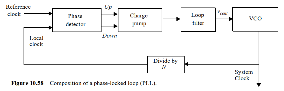
PLL内部结构如下,真正核心的只有两个组件:
- VCO: The voltage-controlled oscillator (VCO) takes an analog control input and generates a clock signal of the desired frequency. VCO接受电压(模拟信号),转换为频率(数字信号),也就是说,VCO使输出频率是电压的函数(非线性)。Charge pump是控制电压增加和减少的模块,Loop filter是低通滤波器,过滤掉电压信号中的高频正弦噪声,使VCO的输入更“纯粹”(减少毛刺信号,jittery clock)
- Phase Detectors: 为什么带s ? 因为可以有两种实现:XOR Phase Detector 和 Phase-Frequency Detector ,Phase Detectors是相位和频率同步的核心,具体原理下面讲
XOR Phase Detector
用一个异或门(XOR)就能实现相位检测,是最简单但有缺陷的实现:
当ref clock和local clock(反馈时钟)有相位差,异或之后输出的就是相位差信号(phase error),这个信号经过线性函数转换成Vdd, 作为VCO的控制电压。
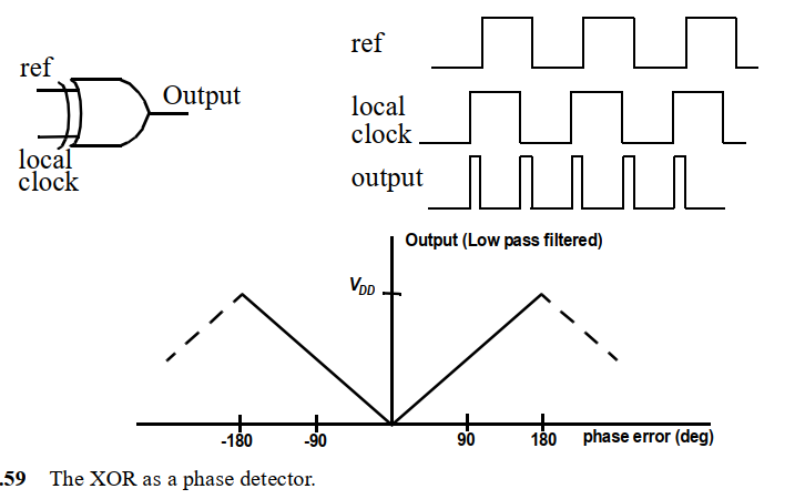
XOR的缺陷:当local clock相位和ref clock相位一致,但local clock频率是ref clock的N倍时,XOR检不输出相位差,但此时PLL输出频率不是预期的频率,而是N倍的预期频率。
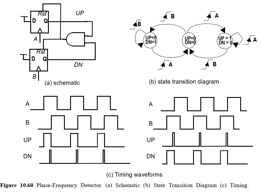
Phase-Frequency Detector (PFD)
为了解决XOR的缺陷,引入了Phase-Frequency Detector (PFD),看名字就知道,它同时检测相位和频率,以保证PLL输出的正确性
如下图,UP/DN是控制VCO的信号,用于给VCO加压/降压;A和B是local clock和ref clock;
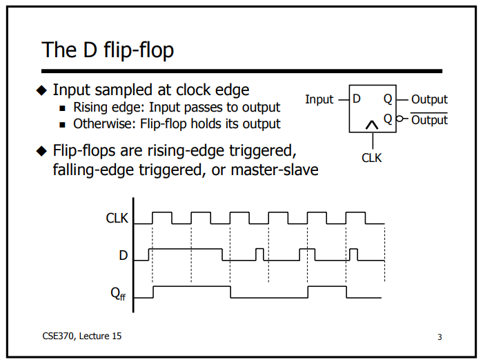
PFD使用触发器(flip-flops),将UP/DN变成A和B的状态机;关于flip-flops的特性,参考 Overview The D latch - University of Washington
(1) PFD如何检测相位差
以左侧信号为例,过程如下:
- 信号A相位超前于信号B, A上升沿时会触发UP信号输出(D触发器特性,这里A作为D触发器的CLK输入信号);
- 当信号B上升沿变化时, B处的触发器也输出DN脉冲,两个触发器的输出都为1,经过与门后Rst复位信号为1,导致A和B的触发器都被reset, 之后UP和DN都变为低;
- 综合下来看,UP信号的宽度就等于相位差,线性转换后就可以作为控制VCO的电压
右侧波形同理,信号A相位落后于信号B,DN即相位差
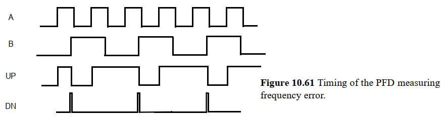
(2) PFD如何检测频率差
如下图,当B频率比A低,PFD输出更多的UP信号增加VCO电压,提高B的频率;当B频率比A高则相反,PFD输出更多DN信号降低B的频率
PLL的指标
PLL structure is a feedback structure and the addition of extra phase shifts, as is done by a high-order filter, may result in instability.
PLL是能造成相位偏移(矫正)的反馈电路,既然是反馈就得像数学求极限一样不断趋近,这决定PLL不是一上电就能马上稳定工作,因此引入PLL的关键指标如下:
Important properties of a PLL are:
lock range—the range of input frequencies over which the loop can maintain functionality; PLL能接受的输入时钟不可能太高,一般是OSC晶振低频时钟。想象一下,太高的输入时钟要去同步相位和倍频,对VCO和相位检测器的精度要求也极高
the lock time—the time it takes for the PLL to lock onto a given input signal; PLL是反馈环路电路,需要不断递归趋近于目标时钟信号直到稳定,稳定需要的时间称为PLL锁定时间
jitter. 毛刺信号,在模拟端称为noise(VCO输入电压),在数字端称为jitter毛刺(VCO输出时钟),这是时钟信号相关模块必不可少的指标
PLL的稳定过程
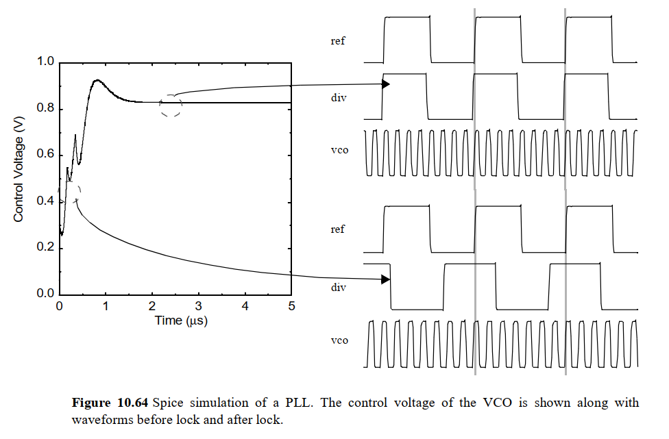
如下图是Spice 仿真将100Mhz reference clock倍频8倍,VCO最终稳定输出800Mhz system clock的过程:
左侧是VCO控制电压,经过几次反馈调整后最终稳定
右侧是时钟信号,ref是输入的100Mhz reference clock,vco是输出的system clock, div是vco输出8分频后的反馈时钟
可见PLL稳定过程是将ref,vco和div时钟信号的相位、频率都收敛到一致
PLL在IC设计IP的实例
以SMIC的PLL IP S65NLLPLLGS 为例介绍实际IC设计中的PLL模块:
(1) 简介
This PLL is developed as an IP block to reduce time to market, risk and cost in the
development of Analog Front –End design. This macro cell is mainly for the clock
generator. It can generate stable high-speed clock from a slower clock signal with
single power supply. The output frequency is adjustable and can be up to 1500MHz.
This PLL integrates a Phase Frequency Detector (PFD), a Low Pass Filter (LPF), a
Voltage Controlled Oscillator and other associated circuit. All fundamental building
blocks as well as fully programmable dividers are integrated in the core. It is useful
for clock multiplication of stable crystal oscillator sources and for de-skew clock
signals
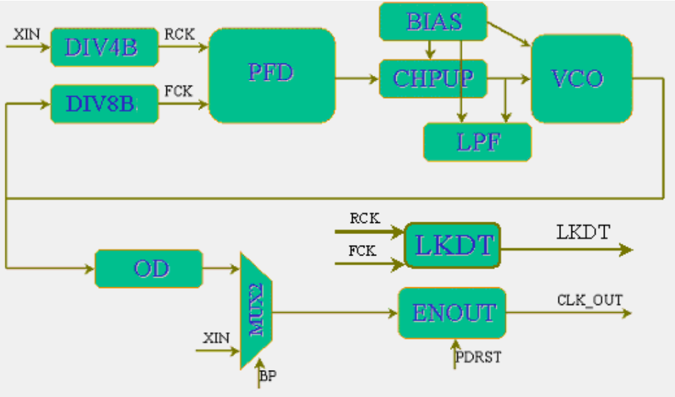
可见主要模块还是PFD + VCO,输出时钟加了一些逻辑门控制,例如PDRST是PLL时钟复位控制。
(2) 主要参数
Technology: SMIC 65nm logic LL process
PFD comparison frequency range from 1Mhz to 50Mhz.
Output clock frequency range from 62.5MHz to 1500MHz
基本体现了PLL的指标:输入输出时钟频率有限制
(3) PLL reset
PLL作为实际可用的模块,其输出频率一定是可调的,以下PLL IP的pin中的M, N即调整频率;对于固件、驱动软件开发者,M,N分频的访问接口是作为寄存器来动态配置。
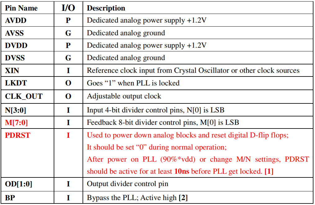
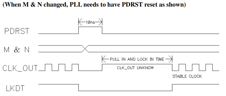
在M,N调整分配时,必须reset PLL并等待PLL再次稳定(PLL lock time),如下图:
LKDT: Lock Detection, 表示目前PLL正在lock,即反映PLL是否处于不稳定状态
PLL在外设时钟配置的实例
SD控制器(SD host)是SOC中常用的外围模块,通过SD specification规定的SD Command通信格式向SD卡通信。
下面以SD host/card的时钟初始化为例,介绍PLL的lock time在外设时钟初始化的影响
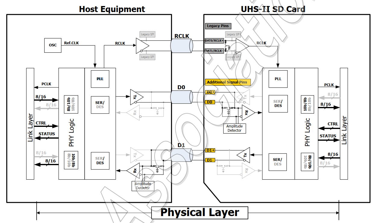
(1) SD 4.0标准的host和card的物理框图如下图,这里重点关注host侧的时钟相关的模块:
- OSC: host 的时钟来源,同时也是PLL的输入
- PLL: host的倍频器,为了给SD UHS-II card提供更高速的工作时钟(UHS-I低速SD card不需要此PLL)
- RCLK: SD card的工作时钟(reference clock)
(2) SD host和card的时钟初始化
SD host和card的时钟初始化包含三步:
1.使能internal clock: sd host chip自己的工作时钟(即base clock,来源是OSC),并等待其稳定,如下图(3)~(4)
2.enable PLL,并等待其稳定,这个等待稳定超时时间为150ms ,如下图(5)~(6)。
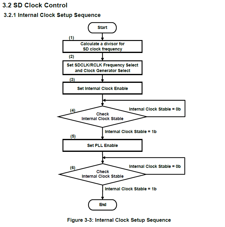
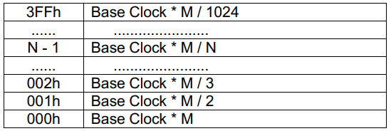
3.待host PLL输出稳定后,即可enable SD clock开始对SD卡供应reference clock时钟, 注意SD clock是下图(1)~(2)就已经计算好的,如下表Base Clock为internal clock,M可理解为PLL倍频后的频率, 经过2^N分频后给SD card作为reference clock。
PLL在电源管理的实例
所谓电源管理,通俗的讲就是按需管理电源:
- 按需,指的是按应用场景的需求,例如在高性能肯定对应高功耗,各种模块全部开启,且时钟频率拉到最大;而睡眠休眠等模式,有时只需要保留能唤醒系统的时钟就行;
- 管理电源,涉及到供电和时钟:将低功耗情景下不需要用到的模块直接关电,将要用到但速度要求不高的模块进入低速时钟工作。
下面以PCIe的电源管理为例,介绍低功耗状态如何影响PLL的状态
(1)PCIe电源管理基本概念
PCIe的电源管理基本概念参考 PCI EXPRESS ARCHITECTURE POWER MANAGEMENT, 也可以参考PCIe标准协议PCIe Base Spec
从上到下包含三层:系统电源状态(S),PCIe链路电源状态(L),PCIe设备电源状态(D)
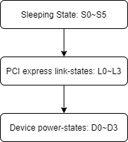
- Sleep state
S0 (Working): This is the active system state in which the platform appears to be “on.”
S1/POS, S1 (Microsoft* OS Stand By): These are the lowest wake latency sleeping states.
S3 (Microsoft OS Stand By) and S4 (Microsoft OS Hibernate): S3 is a low wake latency sleeping state in which all device contexts are lost except system memory
S5 (Microsoft OS Soft-off): In this state, the OS does not save any context and requires a complete OS boot when the system wakes
- Link States
L0: Active state
L1: This link state is a low exit latency link state that is intended to reduce power when the device becomes aware of a lack of outstanding requests or pending transactions
L2/L3 Ready: This link state prepares the PCI Express link for the removal of power and clock.
L3 (link off): Power and clock are removed in this link state
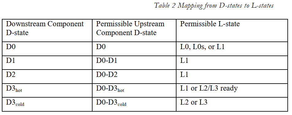
- Device States
D0 (Fully-on): The device is completely active and responsive during this D-state
D1 and D2: There is no universal definition for these D-states. In general, D1 is expected to save
less power but preserve more device context than D2
D3 (Off): Primary power may be fully removed from the device (D3cold), or not removed from the device (D3hot).
S, L, D 三层状态的对应关系如下表
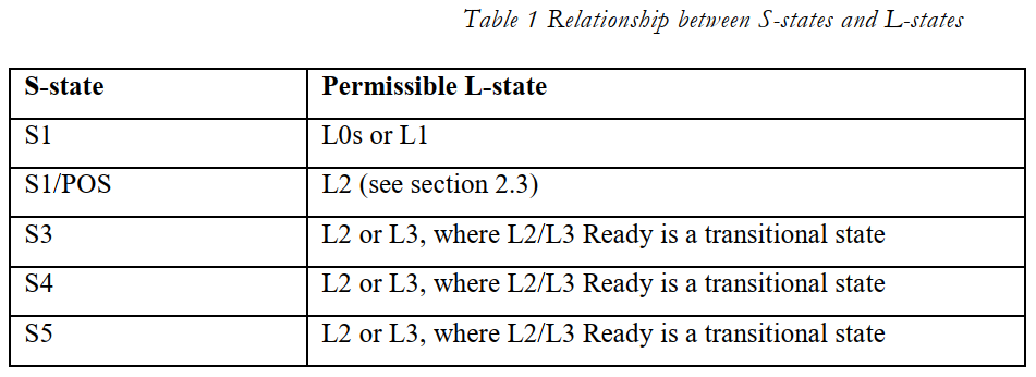
注意,Link state是Sleep state对Device state作用的结果,即状态变化的过程是:
系统发起S3 -> Device sate进入D3->Link state进入L2/L3
(2)使用PLL控制Device state
Device sate进入D3, 设备内部操作即包含PLL的disable,将PLL模块整个关掉,保留OSC低速时钟作为退出D3状态的唤醒时钟源(软件上可以理解为heart beat),当PLL关掉后,其他依赖PLL的高速模块通常也断电,整个设备接近(或彻底)断电,因此设备功耗极低。
Device sate退出D3并进入D0则是相反过程,设备的PLL模块打开,其他依赖PLL的高速模块也打开,整个设备进入Active状态,功耗自然升高。
(3)使用PLL控制Link state
参考chapter11 of Introduction to PCI Express: A Hardware and Software Developer’s Guide
当PCIe link改变时,本质是PCIe时钟改变;PCIe host侧(bridge/Root Complex)的时钟也是低速clock source经PLL倍频后的2.5GHz,如下图:
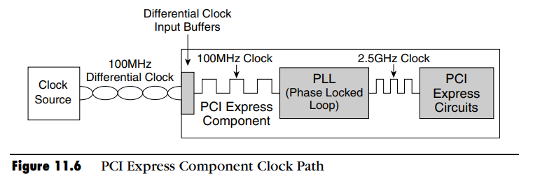
L1 link state的本质:The L1 Link state is an idle state with the internal Phase Lock Loop Circuit turned off. The source clock is still feeding a 100-megahertz differential clock signal to the PCI Express component.
L2 link state的本质:The L2 Link state is an optional auxiliary idle state with the internal Phase Lock Loop Circuit, the external clock source, and the main device power turned off (auxiliary power remains on)
总结就是:PCIe Link State本质是通过关闭PCIe host侧的PLL甚至clock source来实现的。